 |
| Home │ Audio
Home Page |
Copyright © 2012 by Wayne Stegall
Updated March 14, 2012. See Document History at end for
details.
One-Bend Amplifier
Part
1: Compare
a current-feedback
amplifier
allowing
a
one-bend
distortion
characteristic
to
its
voltage-feedback
equivalent.
Introduction
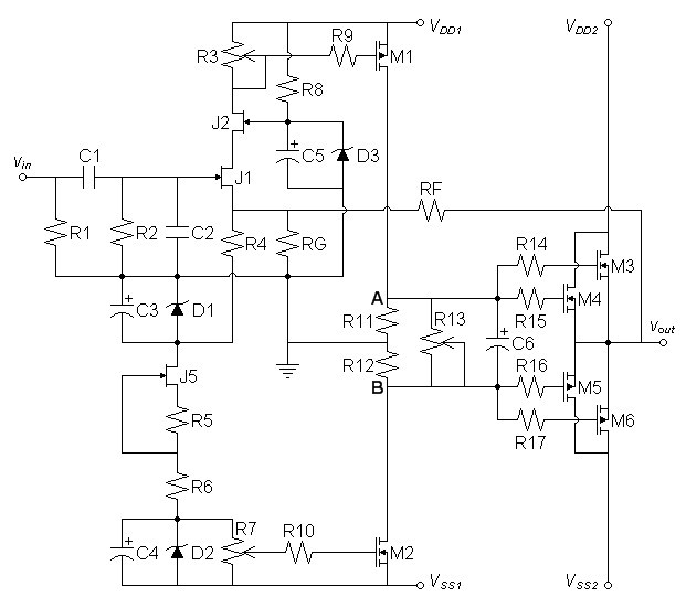
In the article Transfer Curve Shape and Distortion I suggested that a circuit topology that alternated device polarity might produce a euphonic distortion result by bending the transfer curve in only one direction. I decided to compare a useful design using this approach to its similar more common alternative.The One-bend circuit
The complete schematic may obscure the principle. Therefore, look
at J1, M1, and M3-M6. Only they affect the transfer curve.
J2 is only a casode, and M2 a current source. J1 bends the
transfer curve, M1 bends it the same way. Square-law cancellation
dictates that the source follower on the output has the bend of one
MOSFET in the direction of the bank of FETs M3-M4 or M5-M6 which has
the greatest transconductance. NMOS transistors usually have the
greatest transconductance of comparable NMOS and PMOS choices that
might be paired up in this way. On this presumption, the output
stage also bends the transfer curve in the same direction as J1 and M1
did. Then feedback will straighten the one bend to a nice, low,
euphonic distortion result.| Figure 1: Class-a,
three-stage, current-feedback FET amplifier. |
 |
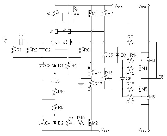
Its common sibling
The comparison circuit is identical except that the two-bend
differential
input stage will complicate the one-bend tendencies of the remainder of
the circuit.| Figure 2: Class-a, three-stage, voltage-feedback FET amplifier. |
 |
Common Design Decisions
- On the basis that 48V CT transformers are commonly available, I decided to design the amplifier to produce 32WRMS then derate it to 30W.
- Use zener diodes to eliminate ripple from first and second stage
bias. 6.2 V zeners were selected as closest common values to the
6V
value expected to have no temperature drift. Cascode bias is set
to 15V.
- Bias first stage to approximately 1mA per JFET.
- Bias second stage to dissipate an average of 1.5W in each of M1 and M2 (45mA).
- Output stage bias to be adjusted to 1A-4A depending on actual circuit and thermal conditions.
Power Supply Design
I decided to split the power supplies to allow the first and second
stages to have much less ripple than the output stage. This
resulted in the following power supply design.| Figure 3: Split power
supply for both circuits. |
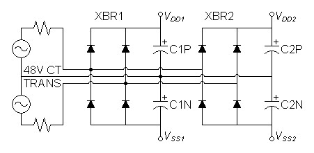 |
The current out of VDD1 and VSS1 average at most 47mA with peak 94mA from VSS1. For no more than average 0.1V ripple
| C1P and C1N ≥ | i
fΔv |
= |
47mA
120Hz × 0.1V |
= 3.917mF |
It is a property of enhancement MOSFETs that they will not leave current mode for linear mode under any conditions until VDS drops below VGS-VT. Since ripple for the first two stages has been specified very low, ripple in the output stage should be filtered by the drain until it exceeds VT a value typically >3V. Allowing 3V of ripple on dynamic peaks would specify less for continuous operation and be entirely acceptable. That simulation showed clipping 5V before rail voltage suggests more ripple headroom in the output circuit than this calculation.
The current out of VDD2 and VSS2 peak at most 8A during dynamic peaks. For no more than average 3V ripple
| C2P and C2N ≥ | i
fΔv |
= |
8A
120Hz × 3V |
= 22.22mF |
Circuit Adjustments
Much of the circuit is adjusted rather than having a calculated bias.- Choose a value for R5 that will bias J5 for 10-12.5mA
before assembly,
- Set R3, R7, and R13 so that the transistors they bias are initially cutoff.
- Connect Node A to ground through a jumper.
- Connect Node B to ground through an ammeter.
- Adjust R7 until ammeter reads 45mA.
- Connect Node B to ground through a jumper.
- Connect Node A to ground through an ammeter.
- Adjust R3 until ammeter reads 45mA.
- Remove jumpers from nodes A and B
- Adjust R13 for desired output bias current.
- Adjust R3 for 0V DC offset.
- Repeat steps 10 and 11 until they both measure correctly.
SPICE Results
At first I intended to alter the open loop gain by trimming R11 and R12
of each circuit until they had comparable distortion levels to base the
comparison. However, I found odd changes in the voltage-feedback
transfer curve that called for a wider comparison.SPICE deck for cfb circuit.
SPICE deck for vfb circuit.
SPICE deck for power supply
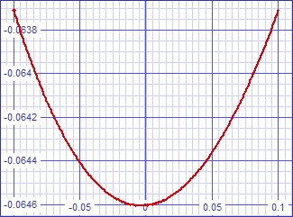
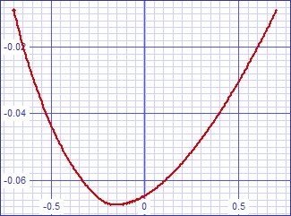
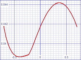
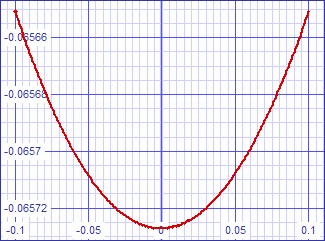
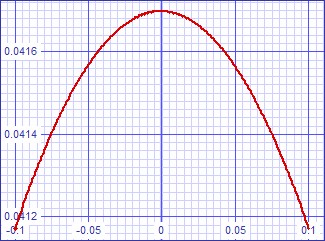
Transfer Error Curves
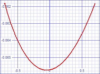
Any localized sharp kinks in these curves are due to localized difficulties in SPICE convergence. You should imagine them to all be smooth. All transfer curves were generated using idealized power supplies because DC analysis removes any capacitive filtering of simulated real supplies.| Figure 4 |
Current feedback |
Voltage feedback |
| Low Feedback Small Signal R11=R12=1.5kΩ |
 |
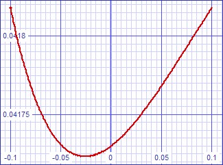 |
| Low Feedback Large Signal R11=R12=1.5kΩ |
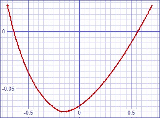 |
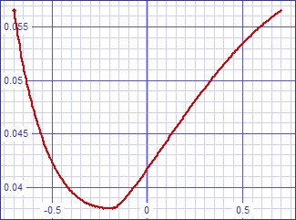 |
| Current feedback | Voltage feedback | |
| Medium Feedback Small Signal R11=R12=1.8kΩ |
 |
|
| Medium Feedback Large Signal R11=R12=1.8kΩ |
 |
 |
| Current feedback | Voltage feedback | |
| High Feedback Small Signal R11=R12=6kΩ |
 |
 |
| High Feedback Large Signal R11=R12=6kΩ |
 |
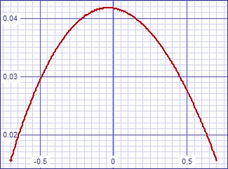 |
Analysis of Transfer Error Curves
- The current-feedback design wins first on the basis of consistency. Both designs appear capable of a desirable, single bend transfer curve. The current-feedback curves always have one positive bend. This is the predictable result of all bending devices bending in the same direction. The voltage-feedback curves start with one-positive bend at low open-loop gains, progress through a two bend curve, to a negative one-bend curve. In a real context of unpredictable device gain, the distortion characteristic of the voltage-feedback circuit is unpredictable.
- That lower signal levels achieve a more parabolic result, where there is a tendency to a parabola at all, is due to the different rate at which higher order terms decrease with level.
- That greater open-loop gain achieves more parabolic results is
due to the diminishing of the differential signal at the input with
increasing feedback. This effect is related to the same effect
with respect to overall signal level.
Fourier analysis for current-feedback circuit, gain matched to distortion of following voltage-feedback analysis, 1W into 8Ω.
Fourier analysis for vout:
No. Harmonics: 16, THD: 0.00623235 %, Gridsize: 200, Interpolation Degree: 3
| Harmonic | Frequency | |
Magnitude | |
Norm.Mag | |
Percent | |
Decibels |
|
|
|
|
|
|
|
||||
| 1 | 1000 | 4.02368 | 1 | 100 | 0 | ||||
| 2 | 2000 | 0.000250739 | 6.23159e-05 | 0.00623159 | -84.1080 | ||||
| 3 | 3000 | 3.9235e-06 | 9.75101e-07 | 9.75101e-05 | -120.219 | ||||
| 4 | 4000 | 9.4909e-08 | 2.35876e-08 | 2.35876e-06 | -152.546 | ||||
| 5 | 5000 | 1.24382e-08 | 3.09125e-09 | 3.09125e-07 | -170.197 | ||||
| 6 | 6000 | 1.7024e-08 | 4.23094e-09 | 4.23094e-07 | -167.471 | ||||
| 7 | 7000 | 1.2994e-08 | 3.22939e-09 | 3.22939e-07 | -169.817 | ||||
| 8 | 8000 | 1.87858e-08 | 4.66881e-09 | 4.66881e-07 | -166.615 | ||||
| 9 | 9000 | 1.22738e-08 | 3.05039e-09 | 3.05039e-07 | -170.312 | ||||
| 10 | 10000 | 1.65326e-08 | 4.10884e-09 | 4.10884e-07 | -167.725 | ||||
| 11 | 11000 | 8.43652e-09 | 2.09672e-09 | 2.09672e-07 | -173.569 | ||||
| 12 | 12000 | 1.52337e-08 | 3.78601e-09 | 3.78601e-07 | -168.436 | ||||
| 13 | 13000 | 1.01237e-08 | 2.51604e-09 | 2.51604e-07 | -171.985 | ||||
| 14 | 14000 | 1.36079e-08 | 3.38196e-09 | 3.38196e-07 | -169.416 | ||||
| 15 | 15000 | 8.07009e-09 | 2.00565e-09 | 2.00565e-07 | -173.954 |
Fourier analysis for voltage-feedback circuit, medium open-loop gain, 1W into 8Ω
Fourier analysis for vout:
No. Harmonics: 16, THD: 0.00667249 %, Gridsize: 200, Interpolation Degree: 3
| Harmonic | Frequency | |
Magnitude | |
Norm. Mag | |
Percent | |
Decibels |
|
|
|
|
|
|
|
||||
| 1 | 1000 | 4.10897 | 1 | 100 | 0 | ||||
| 2 | 2000 | 0.000274035 | 6.66919E-05 | 0.00666919 | -83.5185, | ||||
| 3 | 3000 | 8.61175E-06 | 2.09584E-06 | 0.000209584 | -113.572 | ||||
| 4 | 4000 | 3.15514E-07 | 7.67865E-08 | 7.67865E-06 | -142.294 | ||||
| 5 | 5000 | 2.111E-08 | 5.13754E-09 | 5.13754E-07 | -165.784 | ||||
| 6 | 6000 | 4.68468E-09 | 1.14011E-09 | 1.14011E-07 | -178.861 | ||||
| 7 | 7000 | 1.28597E-08 | 3.12966E-09 | 3.12966E-07 | -170.090 | ||||
| 8 | 8000 | 7.86997E-09 | 1.91531E-09 | 1.91531E-07 | -174.355 | ||||
| 9 | 9000 | 3.98815E-09 | 9.70597E-10 | 9.70597E-08 | -180.259 | ||||
| 10 | 10000 | 2.53434E-09 | 6.16781E-10 | 6.16781E-08 | -184.197 | ||||
| 11 | 11000 | 5.24857E-09 | 1.27734E-09 | 1.27734E-07 | -177.873 | ||||
| 12 | 12000 | 4.42277E-09 | 1.07637E-09 | 1.07637E-07 | -179.360 | ||||
| 13 | 13000 | 3.99287E-09 | 9.71743E-10 | 9.71743E-08 | -180.248 | ||||
| 14 | 14000 | 6.1974E-09 | 1.50826E-09 | 1.50826E-07 | -176.430 | ||||
| 15 | 15000 | 2.35759E-09 | 5.73765E-10 | 5.73765E-08 | -184.825 |
Caveats
Although I did these designs mainly to illustrate a point, a lot care went into their correctness. In spite of this, some things are or may be incomplete.- The slew limiting capacitor C2 is yet to be calculated because I have not yet done that analysis.
- An output protection circuit is omitted for simplicity and because some prefer other means of protection rather than the common safe-operating-area (SOA) limiters for fear of adding distortion.
- The noise analysis was inconsistent: the output noise was
lower than the input noise. Therefore, there is no way of knowing
the affect on noise level of using low-power power transistors in the
second stage. They are expected to have low thermal noise due to
high transconductance but flicker noise may be another matter.
Correction
By accident these simulations were done with the kp of the PMOS transistors of the output stage 5% greater than that of the kn of the matching NMOS transistors. This is near to simulating square-law distortion cancellation and seems not to have affected the outcome of the experiment. In next article, I adjust kn up 5% and kp down by the same amount as would simulate hand choosing transconductance factors favoring an overall NMOS characteristic.This mistake is due to a shortsighted presumption that the KP SPICE parameter was equivalent to kn and kp. I had my SPICE book handy and should have known better. Transconductance factors are calculated properly by the following formula:
| kn or kp = |
KP × W
2 × Leff |
Links
Next article: One-Bend Amplifier March 14, 2012. Part 2: Improving important details of a current-feedback amplifier.|
|
Document History
January 31, 2012 Created.
January 31, 2012 Added another step to circuit adjustments.
March 14, 2012 Added correction concerning output stage
transconductance factor and added a link to next article.