 |
| Home │ Audio
Home Page |
Copyright © 2008, 2009, 2010, 2011, 2014, 2015
Updated November 28, 2015. See document history at
end for details.
SPICE verified where indicated.
Phono Equalization Calculations
Maximize your browser to allow room for the equations. Verified on Internet Explorer and Firefox browsers.
The s variable will
represent seconds or the Laplace s-domain variable according to context.
Table of Contents
Introduction
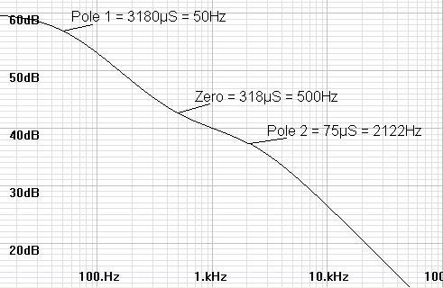
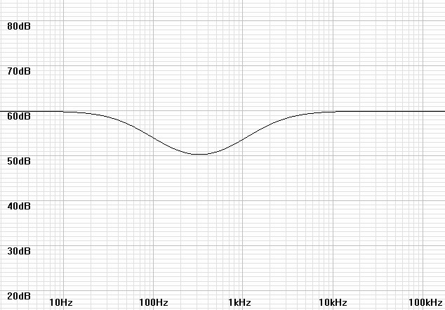
The intention of this document is to give the audio hobbyist mathematical basis to calculate the resistor and capacitor values in the RIAA equalization network of a phono preamp. I searched the internet for this same information and could not find it. As a result my curiosity compelled me to make the calculations myself. The bode plot shown is of typical equalization curve with poles at 3180µs and 75µs, and a zero at 318µs. A Gain of 60dB at DC and 40dB at 1kHz is typical of a MM voltage amplification stage. Many hold that an additional zero at 3.18µs will compensate for a corresponding pole used in phono cutting amplifiers to put a practical limit on the pre-equalization gain at 50kHz.
Typical RIAA Equalization Bode Plot |
|
|
The design cycle involves initially calculating capacitances
from resistors appropriate for the desired gain and noise, rechoosing
the nearest appropriate standard capacitor values in the correct ratio,
then recalculating the resistances from which the nearest standard
values are chosen. This is because resistors are available in
tighter tolerances than are capacitors.
I presume for now that you know how to set the gain for these circuits and that calculating the RC networks are the difficult calculation.
Op amps are used for ease of illustration only. There is no intent to disparage discrete circuit designs.
A Word Concerning Gain
Most calculations are done with regard to low frequency gain (<50Hz). Gain at 1kHz is roughly 1/10 (-20dB) that of low frequency gain. Although you can work well with this ratio, if you desire to set an exact gain at 1kHz use the following ratios instead.| AV-1kHz
AV<50Hz |
= |
0.10103 | (-19.911018dB) |
| AV<50Hz
AV-1kHz |
= |
9.89808 | (19.911018dB) |
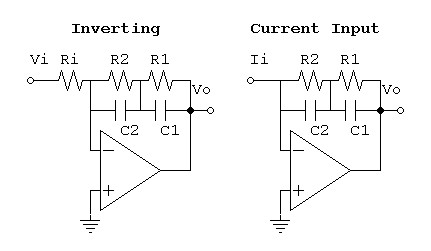
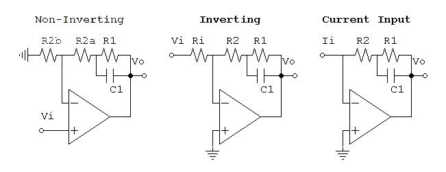
Inverting RIAA Network
(Series-Parallel)
Application
This calculation applies to an RIAA impedance network that converts unequalized signal current into equalized output voltage. This includes inverting and current input stages.
Summary
|
|
TP1 = R1C1 = 3180µs
TP2 = R2C2 = 75µs
TZ = (R1||R2)(C1+C2)
=
318µs
TZ is met when:
R1/R2 ratio = 11.78
and when C1/C2 ratio = 3.6
Inverting series-parallel version verified by SPICE: Model.
Derivation
| (1) |
Z = R1||(1/sC1) + R2||(1/sC2) = | 1
1/R1 + sC1 |
+ |
1
1/R2 + sC2 |
= |
R1
sR1C1+1 |
+ |
R2
sR2C2+1 |
| (2) |
Z = | sR1R2C2
+ R1
+ sR1R2C1
+ R2
(sR1C1 + 1)(sR2C2 + 1) |
Time constant of reduced term is seen in (sT + 1).
Poles are clear, solve for zero.
| (3) |
sR1R2C2 + R1 + sR1R2C1 + R2 = s(R1R2C2 + R1R2C1) + (R1 + R2) |
| (4) |
TZ = | R1R2C2
+ R1R2C1
R1 + R2 |
= |
R1(75µs) + R2(3180µs)
R1 + R2 |
= 318µs |
| (5) |
R1(75µs) + R2(3180µs) = (R1+R2)318µs |
| (6) |
R1(75µs-318µs) + R2(3180µs-318µs) = 0 |
| (7) |
R1
R2 |
= |
3180µs – 318µs
318µs - 75µs |
= 11.777... = 11.7 |
| (8) |
C1
C2 |
= |
TP1/R1
TP2/R2 |
= |
3180µs/11.7R2
75µs/R2 |
= 3.6 |
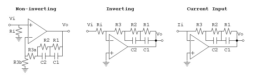
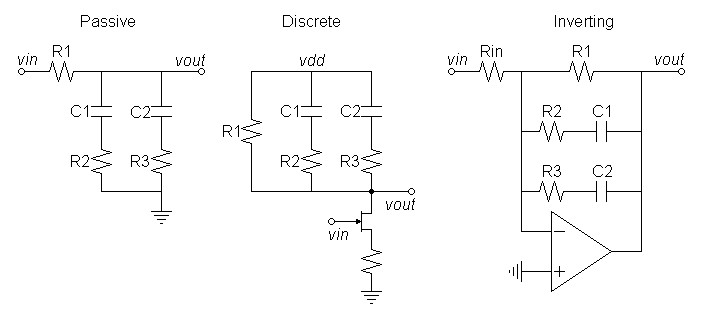
Non-inverting RIAA Network with Extra Zero
(Series-parallel with extra zero)
Application
This calculation applies to an RIAA impedance network typical of non-inverting phono preamplifiers. However it can also be used for inverting and current input applications. An extra zero at 3.18µs requires an extra resistor making it the only network correcting an extra pole alleged to set a practical gain limit in some disk cutters. With a zero at 3.18µs (50kHz) the minimum DC gain is 47dB for the non-inverting circuit. It is worth noting that the non-inverting circuit will always have an extra zero whether you set it to 50kHz or to a maximum frequency. It will be necessary to follow the non-inverting circuit with a first-order lowpass filter of same pole frequency as the undesired zero if you would be rid of it.
Summary
|
|
TP1 = R1C1 = 3180µs
TP2 = R2C2 = 75µs
TZ1 = 318µs
TZ2 = 3.18µs
R1, R2, and R3 in ratio 217.173913 :
17.67514356
: 1 will yield correct
time constants for zeros if C1 and C2 are chosen
to yield correct poles.
| R3b = |
(235.8490566)R3 AV<50Hz |
= (0.2382778)R3
for RIAA
standard 40dB gain at 1kHz |
SPICE model of Inverse RIAA signal generator based on this circuit is verified. (Similar to swapping Ri and RIAA RC network in inverting op-amp circuit to get inverse function. Poles become zeros, and zeros become poles keeping the same time constants).
Inverse RIAA Subckt, Model to Test Inverse RIAA Subckt.
SPICE model of non-inverting series-parallel riaa circuit with extra
zero verifying correct adjustments for gain.
SPICE Model
See Low-noise
Hybrid
Op-amp/Discrete
Phono
Preamp for a complete
design example of this type.
Derivation
| (1) |
Z = R1||(1/sC1) + R2||(1/sC2) + R3 = | R1
sR1C1 + 1 |
+ |
R2
sR2C2 + 1 |
+ R3 |
| (2) |
Z = | sR1R2C2
+
R1 +
sR2R1C1 + R2 + (sR1C1
+
1)(sR2C2 + 1)R3
(sR1C1 + 1)(sR2C2 + 1) |
| (3) |
Z = | sR1R2C2
+
R1 +
sR2R1C1 + R2 + (s2R1C1R2C2
+
sR1C1 + sR2C2 + 1)R3
(sR1C1 + 1)(sR2C2 + 1) |
| (4) |
Z = | sR1R2C2
+
R1 +
sR2R1C1 + R2 + s2R1C1R2C2R3
+ s(R1C1R3 + R2C2R3)
+
R3
(sR1C1 + 1)(sR2C2 + 1) |
| (5) |
Z = | s2R1C1R2C2R3
+ s(R1R2C2 + R2R1C1
+ R1C1R3
+ R2C2R3)
+ (R1 + R2 + R3)
(sR1C1 + 1)(sR2C2 + 1) |
Time constant of reduced term is seen in (sT + 1).
Poles are clear, solve for zeros.
| (6) |
s2R1C1R2C2R3 + s(R1R2C2 + R2R1C1 + R1C1R3 + R2C2R3) + (R1 + R2 + R3) = 0 |
| (7) |
s2(3180µs)(75µs)R3 + s(R1(75µs) + R2(3180µs) + (3180µs)R3 + (75µs)R3) + (R1 + R2 + R3) = 0 |
| (8) |
s2(238.5n(S2))R3 + s((R1 + R3)(75µs) + (R2 + R3)(3180µs)) + (R1 + R2 + R3) = 0 |
| (9) |
s2 |
|
R3(238.5n(S2))
R1 + R2 + R3 |
|
+ s |
|
(R1
+ R3)75µs
+
(R2 + R3)3180µs
R1 + R2 + R3 |
|
+ 1 = 0 |

| (10) |
= s2TZ1TZ2 + s(TZ1 + TZ2) + 1 = 0 |
| (11) |
TZ1TZ2 = | R3(238.5n(s2))
R1 + R2 + R3 |
= 1.01124n(s2) |
| (12) |
R3
R1 + R2 + R3 |
= 4.24m |
| (13) |
R3 = 4.24m(R1 + R2 + R3) |
| (14) |
R1 + R2 + R3 = 235.8490566 R3 |
| (15) |
R1 + R2 = 234.8490566 R3 |
| (16) |
TZ1 + TZ2 = | (R1 + R3)75µs
+
(R2
+ R3)3180µs
R1 + R2 + R3 |
= 321.18µs |
| (17) |
(R1 + R3)75µs + (R2 + R3)3180µs = (R1 + R2 + R3)321.18µs |
| (18) |
R1(75µs - 321.18µs) + R2(3180µs - 321.18µs) + R3(75µs + 3180µs - 321.18µs) = 0 |
(19) R1(-246.18µs) + R2(2858.82µs) + R3(2933.82µs) = 0
| (19) |
R1(-246.18µs) + R2(2858.82µs) + R3(2933.82µs) = 0 |
The two equations (15) and (19) in three variables suggest R1, R2, R3 variable but in fixed ratio as intuition would suggest.
Choose R3 = 1 to solve for this ratio.
Then equation (15) becomes:
(20) R1 + R2 = 234.8490566
Then equation (19)
simplifies to:
(21) R1(-246.18µs) + R2(2858.82µs) =
-2933.82µs
Using simultaneous linear equations (18) and (19), solve for R1 and R2:
| (22) |
Det = |
|
1 -246.18µ |
1 2858.82µ |
|
= 2858.82µ - -246.18µ = 3105µ |

| (23) |
R1 = |
3105µ |
= |
(234.8490566)(
2858.82µ) - -2933.82µ
3105µ |
| (24) |
R1 = 217.173913Ω |
| (25) |
R2 = |
3105µ |
= |
-2933.82µ -
(234.8490566)(-246.18µ)
3105µ |
| (26) |
R2 = 17.67514356Ω |
R1, R2, and R3 in ratio 217.173913
:
17.67514356 : 1 will yield
correct time constants for zeros if C1 and C2 are
chosen to yield
correct poles.
| (27) |
AV<50Hz = |
R1 + R2 + R3a
+
R3b R3b |
= |
(217.173913 + 17.67514356 + 1)R3 R3b |
= |
(235.8490566)R3 R3b |
Solve for R3b to get final gain equation
| (28) |
R3b = |
(235.8490566)R3 AV<50Hz |
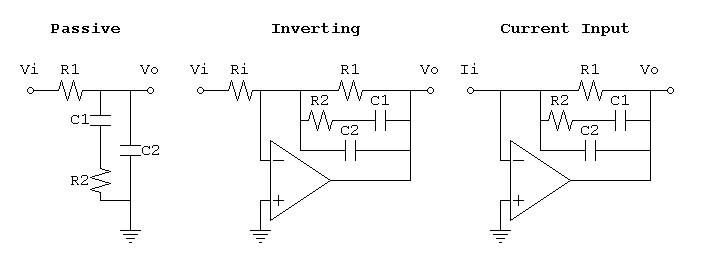
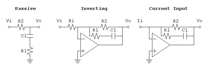
Passive RIAA Network
(Parallel)
Application
This calculation applies to an RIAA network normally used for passive equalization. Parallel topologies are also preferred for discrete transistor designs because stray circuit capacitances can be compensated in C2 and drain/collector resistances in R1. Application of Thevenin’s theorem moves R1 into parallel with C1 and R2, opening up the use of the same network for inverting and current input applications.
Summary
|
|
TP1 = 3180µs
TP2 = 75µs
TZ = 318µs = R2C1
R1C2 = 750µs
R1C1 = 2187µs
R1:R2 = 6.877358491
C1:C2 = 2.916
Passive parallel version verified by SPICE: Model, Inverse RIAA Subckt used in model.
Derivation
| (1) |
Z = R1||(R2+(1/sC1)))||(1/sC2) = |
|
R1 || |
|
sR2C1
+
1
sC1 |
|
|
|| | 1
sC2 |
| (2) |
Z = |
|
1
|
|
|| | 1
sC2 |
= |
|
1
|
|
|| | 1
sC2 |
| (3) |
Z = | sR1R2C1
+
R1
s(R1C1 + R2C1) + 1 |
|| | 1
sC2 |
= |
1
|
| (4) |
Z = | 1
|
| (5) |
Z = | sR1R2C1
+
R1
s2R1R2C1C2 + s(R1C1 + R2C1 + R1C2) + 1 |
Zero is clear:
| (6) |
sTZ + 1 = | sR1R2C1
+
R1
R1 |
, therefore TZ = R2C1 = 318µs |
Solve for poles:
| (7) |
s2TP1TP2 + s(TP1 + TP2) + 1 = 0 |
(8) TP1TP2 = R1R2C1C2 = (R2C1)R1C2 = TZR1C2 (from equations (5) and (7))
| (8) |
TP1TP2 = R1R2C1C2 = (R2C1)R1C2 = TZR1C2 (from equations (5) and (7)) |
| (9) |
R1C2 = | TP1TP2
TZ |
= |
(3180µs)(75µs)
318µs |
= 750µs |
| (10) |
TP1 + TP2 = R1C1 + R2C1 + R1C2 (from equations (5) and (7)) |
| (11) |
3180µs + 75µs = R1C1 + 318µs + 750µs |
| (12) |
R1C1 = 3180µs + 75µs - 318µs - 750µs = 2187µs |
| (13) |
R1
R2 |
= |
R1C1
R2C1 |
= |
2187µs
318µs |
= 6.877358491 |
| (14) |
C1
C2 |
= |
R1C1
R1C2 |
= |
2187µs
750µs |
= 2.916 |
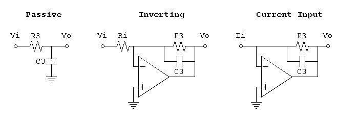
Passive RIAA Network with Extra Zero
(Parallel)
Application
This calculation adds an extra 50kHz zero to an RIAA network
normally used for passive equalization. Parallel topologies are
also preferred for discrete transistor designs because stray circuit
capacitances can be compensated in C2 and drain/collector
resistances
in R1. The addition of R3 in series with C2
to add the
extra zero
somewhat diminishes this advantage, complicating the compensation for
stray capacitance. Application of Thevenin’s theorem moves R1
into parallel with C1 and R2, opening up the use
of the same
network
for inverting and current input applications.
Summary
 |
TP1 = 3180µs
TP2 = 75µs
TZ1 = R2C1 = 318µs
TZ2 = R3C2 = 3.18µs
R1C1 = 2209.09µs
R1C2 = 724.73µs
Resistors R1, R2, and R3 are in ratio 227.902:32.8066:1
Passive parallel version verified by SPICE: Model, Inverse RIAA Subckt used in model.
Derivation
| (1) |
Z = R1 || (R2+1/sC1)
||
(R3 +
1/sC2) = R1 || |
|
sR2C1+1
sC1 |
|
|| |
|
sR3C2+1
sC2 |
|
| (2) | 1 |
1 |
||||||||
| Z = |
|
= |
|
|||||||
|
|
| (3) |
R1(sR2C1+1)(sR3C2+1) | R1(sR2C1+1)(sR3C2+1) | ||
| Z = |
|
= |
|
|
| (s2R2R3C1C2
+
s(R2C1+R3C2) +1) + (s2R1R3C1C2 + sR1C1) + (s2R1R2C1C2 + sR1C2) |
s2(R2R3C1C2+R1R3C1C2+R1R2C1C2)
+ s(R2C1+R3C2+R1C1+R1C2) + 1 |
Zeros are clear:
TZ1 = 318µs = R2C1
TZ2 = 3.18µs = R3C2
Solve for poles in form of
| (4) |
s2TP1TP2
+ s(TP1+TP2) + 1 = 0 |
where
| (5) |
TP1TP2 = R2R3C1C2 + R1R3C1C2 + R1R2C1C2 = TZ1TZ2 + TZ2R1C1 + TZ1R1C2 |
| (6) |
TP1+TP2 = R2C1 + R3C2 + R1C1 + R1C2 = TZ1 + TZ2 + R1C1 + R1C2 |
Let TA = R1C1, TB = R1C2, TP1 = 3180µs, TP2 = 75µs and setup simultaneous linear equations for TA and TB:
From equation (5)
TZ2TA + TZ1TB = TP1TP2 - TZ1TZ2
3.18µTA + 318µTB = (3180µ × 75µ) - (318µ × 3.18µ) = 238.5n - 1.01124n
| (7) |
3.18µTA + 318µTB = 237.489n |
From equation (6)
TA + TB = TP1 + TP2 - TZ1 - TZ2 = 3180µ + 75µ - 318µ - 3.18µ
| (8) |
TA + TB = 2.93382m |
Using simultaneous linear equations (7) and (8), solve for TA and TB:
| (9) |
Det = |
|
3.18µ 1 |
318µ 1 |
|
= 3.18µ – 318µ = –314.82µ |
| (10) |
TA = |
–314.82µ |
= |
237.489n –
(318µ)(2.93382m)
–314.82µ |
| (11) |
TA = 2209.09µs = R1C1 |
| (12) |
TB = |
–314.82µ |
= |
(3.18µ)(2.93382m) – 237.489n
–314.82µ |
| (13) |
TB = 724.73µs = R1C2 |
| (14) |
R1
R3 |
= |
TB
TZ2 |
= |
724.73µs
3.18µs |
= |
227.902 |
| (15) |
R1
R2 |
= |
TA
TZ1 |
= |
2209.09µs
318µs |
= |
6.94682 |
| (16) |
R2
R3 |
= |
R1/R3
R1/R2 |
= |
227.902
6.94682 |
= |
32.8066 |
Resistors R1, R2, and R3 are in ratio 227.902:32.8066:1
Two-Stage RIAA Equalization
Application
Sometimes it is desireable to divide the equalization between two
stages. All practical circuits put the 3180µs pole and the 318µs
zero in one stage leaving the 75µs pole to the other.
| Circuit
1:
Series/Parallel |
 |
Summary
TP1 = R1C1 = 3180µsTZ1 = (R1 || R2)C1 = 318µs
R1 = 9 × R2
R2 = R2a + R2b for non-inverting circuit
Derivation
(1) Z = R2 + (R1||(1/sC1))| (2) |
|
R1 |
sR1R2C1
+
R1 + R2 |
|||||
| Z = R2 + |
|
= R2 + |
|
= |
|
|||
|
sR1C1
+ 1 |
sR1C1
+ 1 |
| (4) |
TZ1 = |
R1R2C1
R1 + R2 |
= (R1 || R2)C1 = 318µs |
(5) TZ1 x 10 = TP1
(6) (R1 || R2)C1 x (TP1/TZ1) = R1C1
(7) (R1 || R2) x (TP1/TZ1) = R1
| (8) |
(TP1/TZ1) | ||||
|
|
= R1 |
||||
|
| (9) |
1
R1 |
+ |
1
R2 |
= |
(TP1/TZ1)
R1 |
, therefore |
1
R2 |
= |
(TP1/TZ1) –
1
R1 |
| (10) |
R1 = |
 |
TP1
TZ1 |
– 1 |
|
R2 |
Substituting back TP1/TZ1 = 10 into equation 10 gives
(11) R1 = 9 × R2
| Circuit
2:
Parallel/Series |
 |
Summary
TP1 = (R2 + R1)C1 = 3180µsTZ1 = R1C1 = 318µs
R2 = 9 × R1
Derivation
(1) Z = R2 || (R1 + 1/sC1)| (2) |
|
sR2R1C1
+
R2 |
|||||||
| Z = |
|
= |
|
||||||
|
s(R2
+ R1)C1
+ 1 |
| (4) |
TZ1
= |
R2R1C1
R2 |
= R1C1 = 318µs |
(5) TP1 =10TZ1
(6) (R2 + R1)C1 = (TP1/TZ1) × R1C1
(7) R2 + R1 = (TP1/TZ1) × R1
| (8) |
R2 = |
|
TP1
TZ1 |
– 1 |
|
R1 |
Substituting back TP1/TZ1 = 10 into equation 8 gives
(9) R2 = 9 × R1
| 75µs
Lowpass
Stage
Common
to
Both |
 |
Summary
TP2 = R3C3 = 75µsIf you have comments on the calculations email me at contact@waynestegall.com
Current Input Networks
Application
The RIAA equalization calculations above presume that no
equalization is needed for the input loop itself. For voltage
input designs, correct RC loading at the preamp input meet these
conditions, although not perfectly. Reading reviews of current
input designs did not mention any special compensation that I
remember. However when I reexamined this issue I found the
following result: The virtual short at the input reduces the
equivalent input loop to a RL response with a low cutoff frequency,
which would greatly attenuate the treble. This is because the
complex pole pair of the full second order circuit diverges into two
real poles below a Q of 0.5 (The second pole is pushed far into the
ultrasonic region with the Q values involved). Therefore it is
necessary to add a zero of the same value to the compensation circuit,
perhaps in a second stage. I present this result only after I
verified it by examining a patent for this type of circuit issued in
1984 (That it expired 17 years later in 2001 makes this a public domain
design.) Because in the winding of an inductor both R and L
increase with the number of turns, cartridges whose windings are made
with the same gauge magnet wire may all have the same or similar RL
response. This suggests the selection of a fixed compensation
zero as a design compromise. Others may want to have an
adjustable zero to tailor the compensation to their desired cartridge.
Summary
Time constant and frequency of pole of cartridge RL response and therefore of required compensation zero:| TZ3 = | L
R |
| fZ3 = | R
2πL |
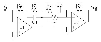
The circuit shown is recommended because it allow adjustable compensation zero to be place in either stage without the adjustment affecting the value of the poles.
| Recommended
circuit
allows
placement
of
compensation
in
either
stage. |
 |
Design equations
For first stage cartridge compensation zero adjusted by R2:
first stage:TP1 = R1C1 = 3180µs
TZ1 = (R1 || R2)C1 = TZ3
| R1 = |
|
3180µs
TZ3 |
– 1 |
|
R2 |
second stage:
TZ2 = (R3 + R4)C2 = 318µs
TP2 = R3C2 = 75µs
R4 = 3.24 × R3
Verifying SPICE model.
Reverse RIAA subcircuit used with all models.
For second stage cartridge compensation zero adjusted by R4:
first stage:TP1 = R1C1 = 3180µs
TZ1 = (R1 || R2)C1 = 318µs
R1 = 9 × R2
second stage:
TZ2 = (R3 + R4)C2 = TZ3
TP2 = R3C2 = 75µs
| R4 = |
|
TZ3
75µs |
– 1 |
|
R3 |
Verifying SPICE model.
Reverse RIAA subcircuit used with all models.
In either case the low frequency transimpedance gain is the same.
| ZGAIN = |
(R1 + R2)R5
R4 |
Which version to choose?
My first instinct was to place the compensation adjustment in the second stage because a potentiometer would contribute less scratch noise there. The drawback is that the adjustment of R4 stands to alter the gain in direct proportion to the alteration in compensation turnover frequency. However, if the compensation zero is placed in the first stage the adjustment of R2 does not stand to alter the gain much so long as the expected condition (R1 >> R2) holds. If the scratching of potentiometers is unwanted in high gain circuits perhaps stepped attenuators should be used with the stipulation that adjustments be made with the preamplifier offline.Other topologies
The first topology was given to allow the adjustable zero to be placed in either stage. However the stage with the fixed zero does not have to be that first given and choosing the alternative gives the additional circuits below. Particularly note that the discrete circuit prefers the series-parallel topology for both stages so that R4 can compensate for the transistor output impedance's effect on the second stage network.| Series-Parallel
in
both
stages
allowed
by
adjustment
in
first
stage |
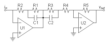 |
| Discrete Full Series-Parallel Circuit |
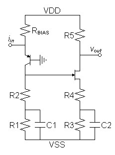 |
| Note: Incomplete
schematic only illustrates equalization topology, biasing is likely
incorrect |
Design equations
For first stage cartridge compensation zero adjusted by R2:
first stage:TP1 = R1C1 = 3180µs
TZ1 = (R1 || R2)C1 = TZ3
| R1 = |
|
3180µs
TZ3 |
– 1 |
|
R2 |
second stage:
TZ2 = R3C2 = 318µs
TP2 = (R3 || R4)C2 = 75µs
R3 = 3.24 × R4
Verifying SPICE model.
Reverse RIAA subcircuit used with all models.
| Parallel-Series in both stages allowed by adjustment in second stage |
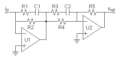 |
For second stage cartridge compensation zero adjusted by R4:
first stage:TZ1 = R1C1 = 318µs
TP1 = (R1 + R2)C1 = 3180µs
R2 = 9 × R1
second stage:
TZ2 = (R3 + R4)C2 = TZ3
TP2 = R3C2 = 75µs
| R4 = |
|
TZ3
75µs |
– 1 |
|
R3 |
Verifying SPICE model.
Reverse RIAA subcircuit used with all models.
Yet more
After giving these additional topologies, more can be specified by swapping the stage 1 network of R1, R2, and C1 with R5. By moving all equalization to the second stage the first stage then gives straight preliminary gain. This approach may be favored for lower noise by the fact that the current-input signal may have much flatter frequency response than that of a voltage input signal as shown the following plot.| Current-input
equalization
at
a
plausibly
typical
cartridge
LR
frequency
of
212.2Hz
shows
much
flatter
equalization
than
voltage input designs. |
 |
Derivation
The derivation of the design equations from the topology and Laplace equations is the same as that for the Two-Stage RIAA Equalization given above. Indeed, the first stage is exactly the same as that of the series-parallel first stage given before. The second stage has a parallel-series RC component on the input side of the op-amp where it was in the feedback loop of the first stage parallel-series that came before thus inverting the transfer equation. This converts poles to zeros and zeros to poles but otherwise the calculations remain the same with minor differences.|
|
Document History:
? 2008 Creation
October 24, 2009 Corrected typo in equation (3b) of Calculating Passive RIAA Equalization
May 7, 2010 Corrected capacitor ratio of Passive RIAA network in summary to match result of calculations.
June 2, 2010 Added two-stage RIAA calculations.
June 22, 2010 Corrected calculations for Calculating Non-inverting RIAA Network with Extra Zero (Series-parallel with extra zero) and verified with SPICE. Verified others with SPICE as well and provided models where indicated. Delete incomplete example at end. All calculations for circuits in this document are deemed correct and verified at this time except that full current input calculations have not been developed.
July 5, 2010 Added section detailing adjustments for exact 1kHz gain relative to that which is approximate.
July 6, 2010 Removed reference to an error corrected long ago.
September 16, 2010 Corrected isolated error in equation (9) of Calculating Non-inverting RIAA Network with Extra Zero that did not affect results because the correct value was carried forward in the calculations instead. In same section make additional calculations to correct incorrect gain presumptions. (SPICE had correctly verified equalization but not gain :-\ )
October 29, 2010 Added link to design example.
March 23, 2011 Added Passive RIAA network with extra zero.
March 23, 2011 Changed second unit from S to s to distinguish it from conductance unit, made other minor improvements.
February 6, 2014 Added schematic and design equations for op-amp based current-input circuit.
March 17, 2014 Expanded derivation of two stage equalization equations to more easily show how current-input equalization derives from them. Added more topologies and detail for current input designs.
November 28, 2015 Improved formatting.